PCB Etching overview with Inkjet and Photoresist Dry Film (Part 1)
DIY intro to etching without using a laser printer
DIY PCB prototyping can be fun especially using recycled and cost effective products. The output is some interesting set of home IoT devices which ehm yes are usefull 😀
I’ll give a brief overview of the complete process using photoresist dry film, it’s not an etching course, maybe could do that in the future. I mainly want to give an idea of costs because some people may think it’s really expensive and I’ll also show final results. Total costs for making a PCB will be reported at the end of the article.
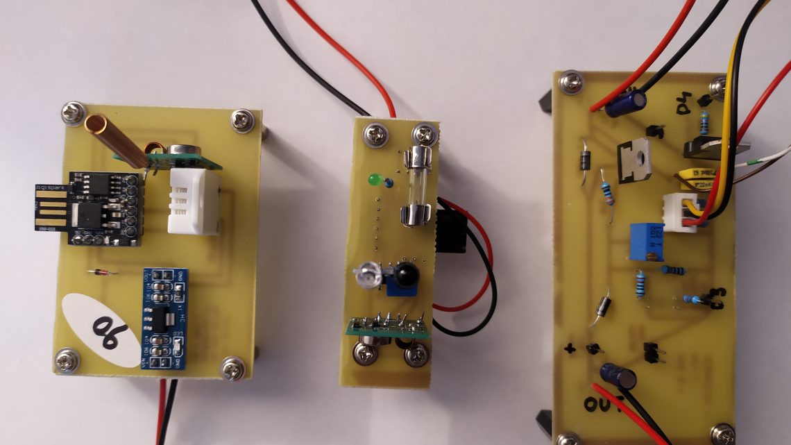
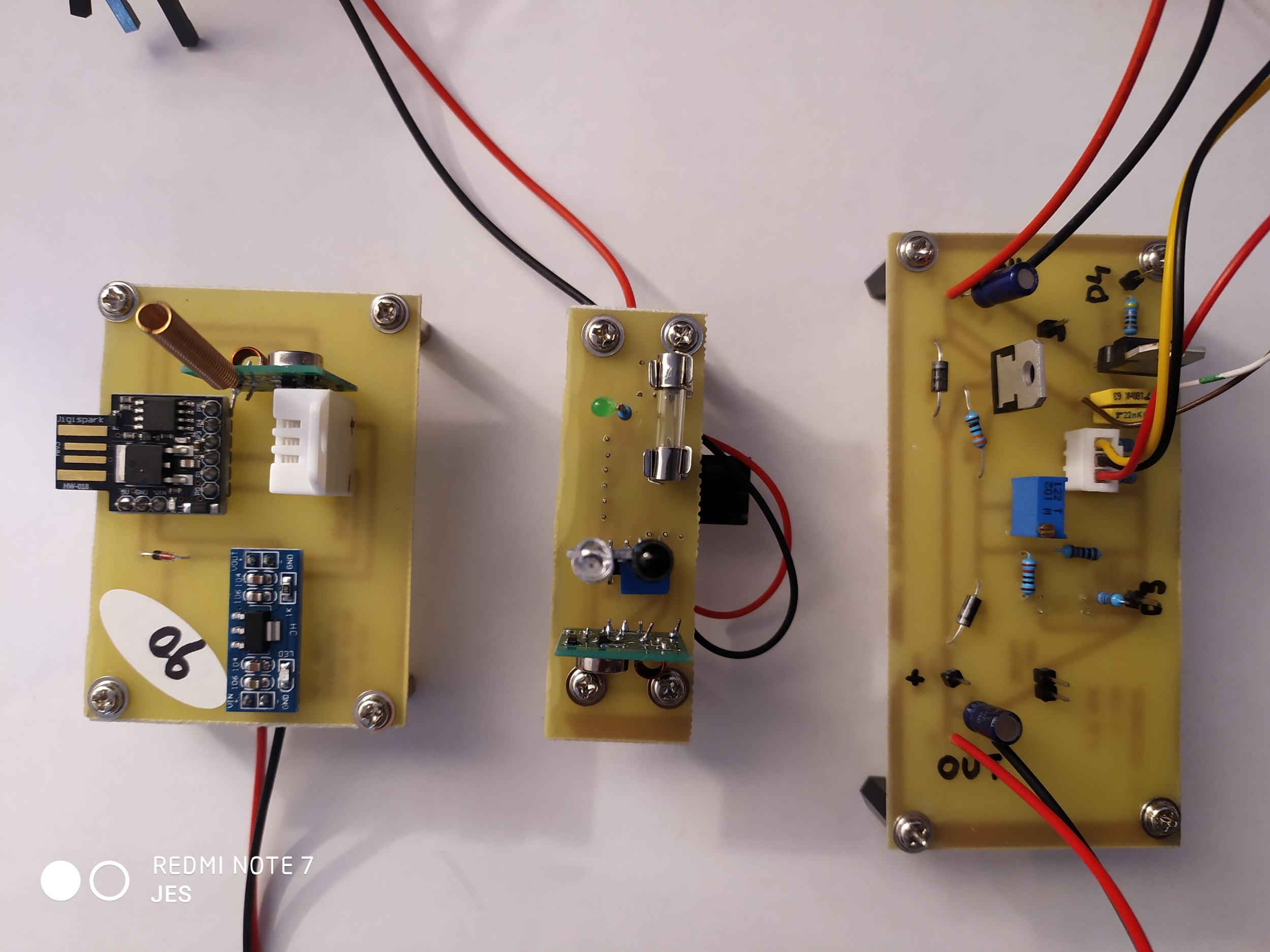
Ok, results first: a lithium battery charger which follows correct datasheet charging curves (the biggest board in photos), an ATTINY based temperature/humidity measurement device (the medium size board) and a touchless switch, again ATTINY based (the smaller board). Both the ATTINY devices send out readings using 433MHz frequency.
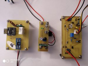
Homemade PCBs
To get some working boards took some time and, I think, many different attempts using acids and all that stuff. I did quite a bit of research and watched many YouTube videos before getting any result, it took me a couple of months studying. I was quite frustrated at the first two attempts because simply the processes showed on the tube didn’t work as expected. The complete process to make a board takes about 30-45 minutes excluding the board designing process itself. You can also make two or more boards at once depending on the size of your copper PCB board.
After designing and preparing the PDF/bitmap/whatever file with the schematics, steps for making a PCB are these:
- Print the master schematics on opaque or transparent paper;
- Use the bromograph to impress design on the copper PCB board;
- Pass the copper PCB board in sodium carbonate;
- Pass the copper PCB board in muriatic acid (concentrated 33%) and hydrogen peroxide (130 volumes);
- Pass the copper PCB board in pure acetone.
Schematics Design
Technical design is made with free Windows software Express PCB (made by ExpressPCB LLC, and, no, I have no connection with them!). I tried different free software, online ones too, but this was the easiest for me. Quick and very easy PCB making with a very fast learning curve, after 30 minutes I was designing my own boards.

Express PCB Software
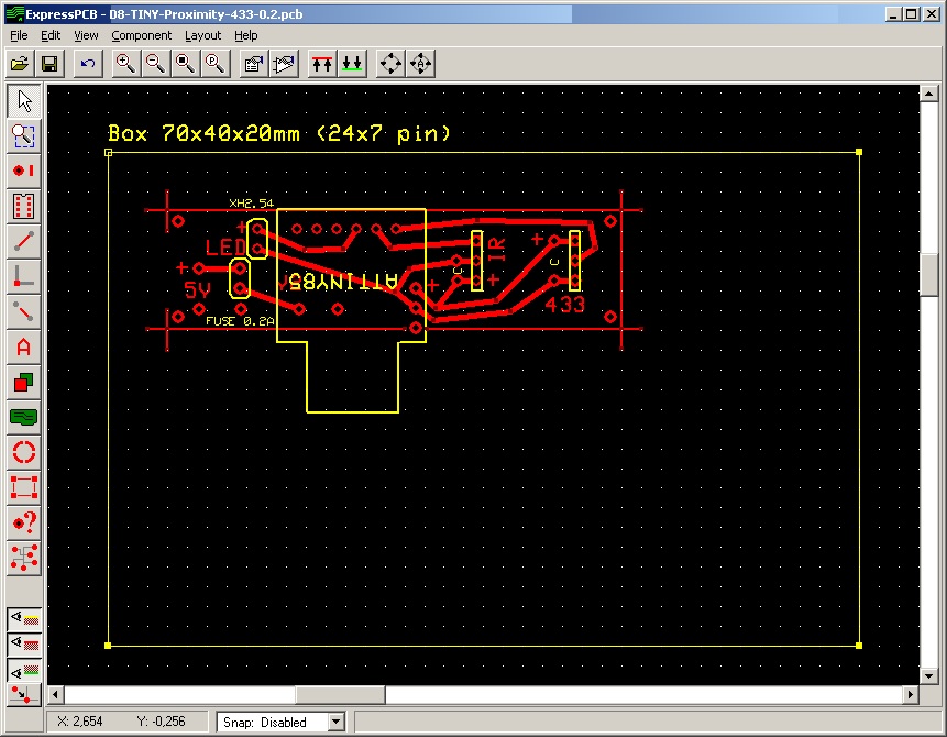
When using components which are not symmetrical requires attention. When we print a PCB with resistors we don’t have any problems but if the component has positive and negative pins, for example, we must remember that soldering will be done on the copper side and components pins will be inserted on the other side.
From ExpressPCB the output I want is a high resolution image or PDF. This program exports to PDF so that’s ok for me.
Print the master schematics
For printing master PCB schematics I use opaque paper (Wintex A4 Tracing Paper 100 sheets, 16€ on Amazon) on an HP Inkjet printer; inkjet isn’t the best choice for printing because black background isn’t a solid black pattern.
Now, this printing stuff can be quite tricky, so lets keep in mind that we should:
- Keep the correct proportion of the picture we print, that is holes must be at the right distance, so I would say don’t use zooming, reducing or fit-to-page functionalities; we can surely say that printing output (in PDF file) from the design program will produce a correct output, so we must be careful in the following steps;
- We must reverse the image and ExpressPCB doesn’t have this feature (black becomes white and viceversa); we can do this with an image processing program, I use GIMP;
- Flipping the image isn’t necessary because printing on transparent paper (or semi-transparent or opacque) means that we don’t need to flip anything; if you feel better working with flipped images just turn the printed paper around;
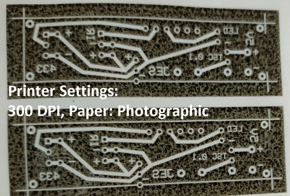
- Injket printers don’t give us a solid black printing but, instead, a blotchy black; so this will require a couple of printing tests to choose the best combination of settings for the printer. I set my HP printer to use maximum DPI, monocromatic print, and I disabled special features which better photo printing;
- We overlap two printouts to get a better black. That means we print two schematics on paper, cut them with scissors leaving an inch margin all around, overlap them and stick them together with tape.
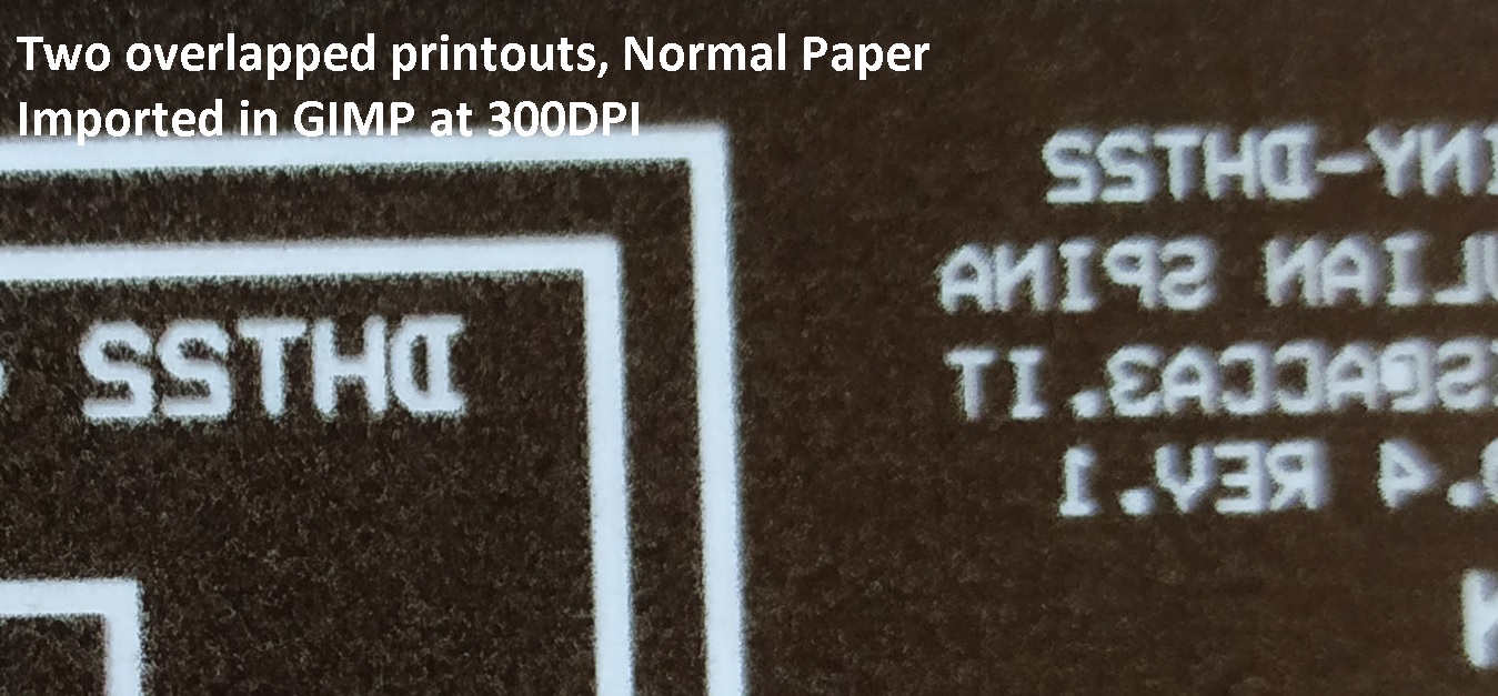
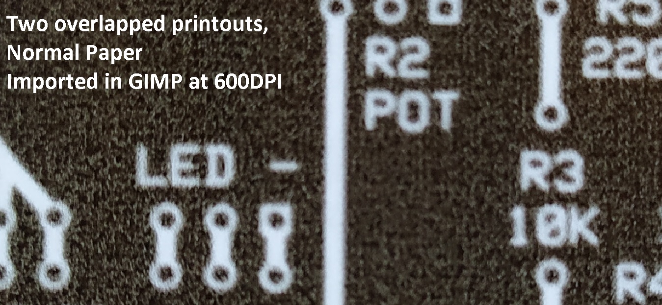
I had best results printing a PDF from ExpressPCB, importing it in GIMP at 300DPI resolution to reverse it and then printing on paper from GIMP choosing “normal paper”.

Now, if you look at the two printing tests you will notice a big difference in output when choosing normal paper VS photographic paper. Setting normal paper gives a more uniform printout while choosing photographic paper gives larger black areas but with a lower granularity. Consider we will overlap and tape together two printouts and choosing normal paper will give a better result. You can check yourself looking at the printouts against a light source.
As for what concerns DPI settings it always best not to touch anything here, hoping that default settings will give a good result. When I import the PDF generated from ExpressPCB into GIMP I can choose the DPI resolution. I tried both 300 and 600DPI and had the best result with 300DPI (I was expecting the opposite!).
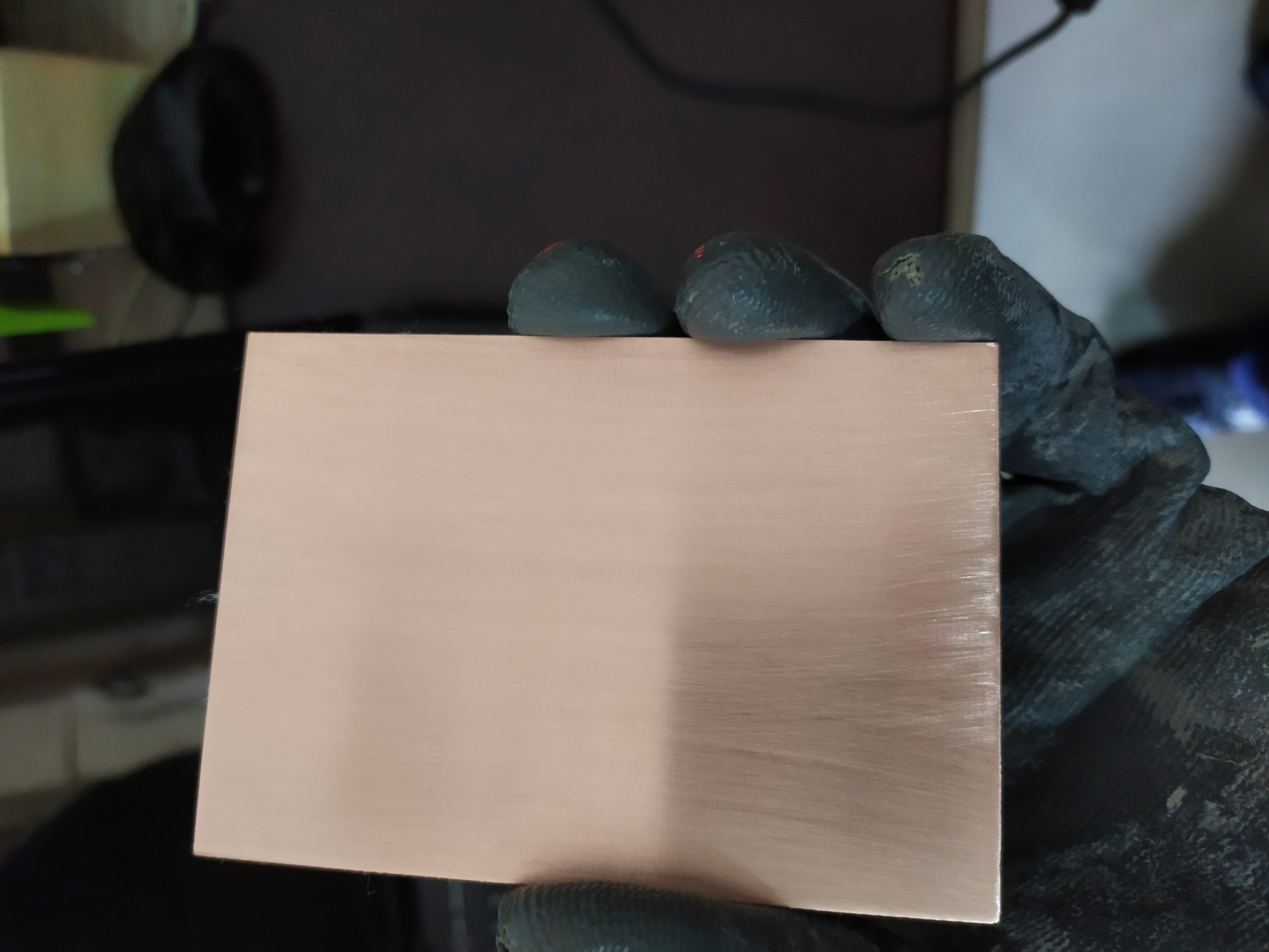
Use the bromograph to impress design
After cleaning the copper board we can proceed with UV impression. I clean the board using a fine sandpaper (I use 400 grane sand paper and it works well, even finer should be ok, too) and then i wash it under tap water and dry it with a cloth. The board should be nice and shiny without any black marks or stains.
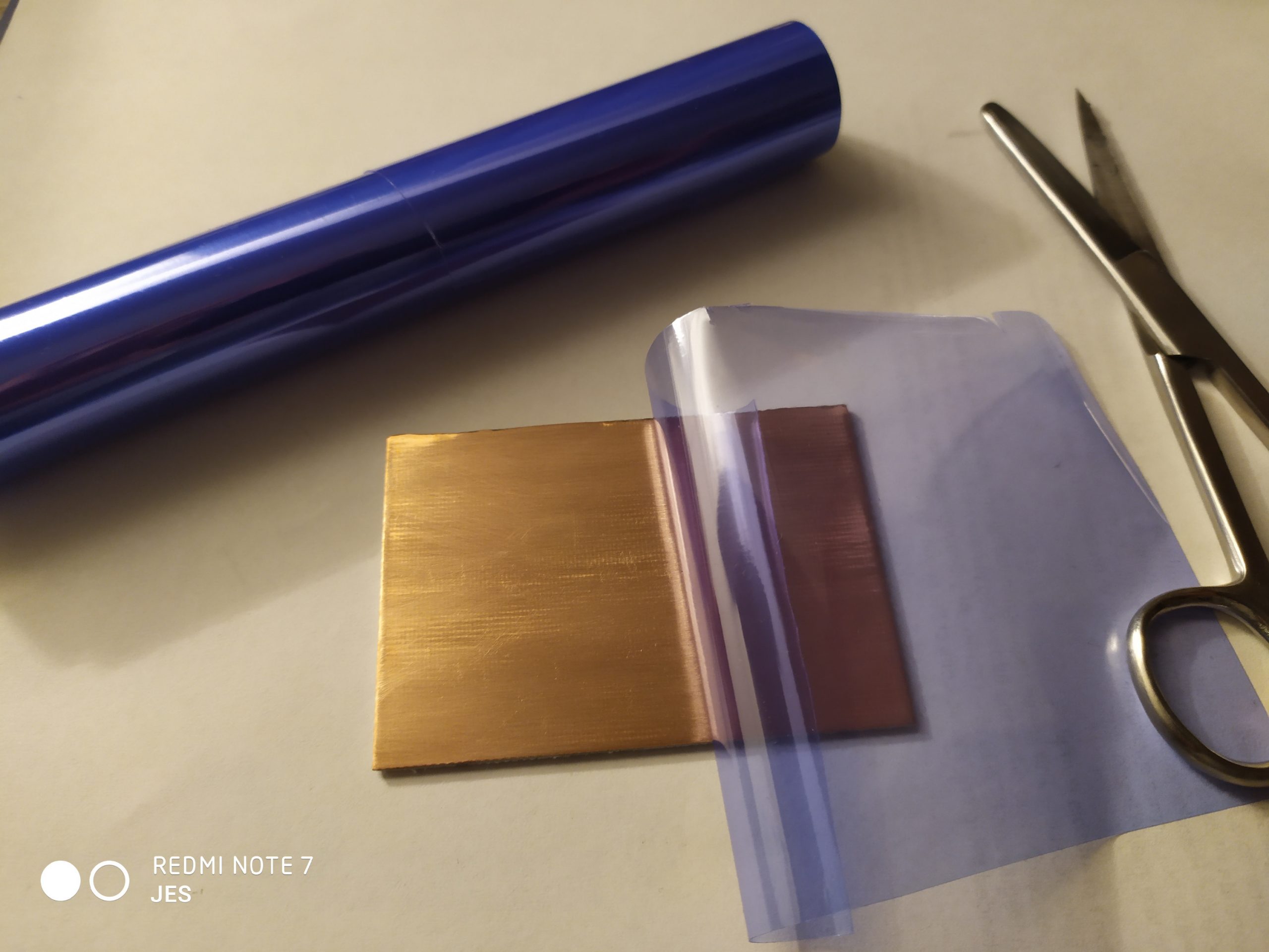
Now that we have our nice and black printout we can “cook it” in the bromograph which will impress the image on the copper board using UV light. Cut a square of photoresist dry film leaving an inch margin all around and apply it on the copper PCB board; you must remove the transparent protective layer and apply the sticky side on the board. This step will work easy after you do it a couple of times because no air bubbles must be between the film and the board. To remove the transparent film I go better sticking two little squares of tape on a corner of the film (one on top and one on the bottom) and pulling them to remove.

Cut a square of film 
Remove protection and Apply film
On Youtube videos you’ll see people using a hairdryer or an iron to make a better contact of the film (which is sort of rubbery) on the board. I tried both methods and ended up with a badly melted film which could not be used. If something goes wrong in this phase we can remove the film from board using pure acetone and start over again with applying the film. So what I do is: I apply the film to the board after removing the transparent protection; put a white A4 paper on the board to avoid direct contact of iron base with the dry film; switch my iron on, set on lowest temperature, and when it’s still not too hot, lets say after 10-15 seconds, iron it for 5-10 seconds. More than that and the dry film will melt and we’ll have to start over again. The result must be without bubbles or melted parts.
My bromograph is home made using an old wooden box, 100 UV leds (model 2835, not 3825!) cut into 5 strips of 20 leds each and glued to a plastic board. Current comes from a little DC-DC converter board which accepts up to 30V in input and you can regulate output voltage; I set it to 14.3V because I measured voltage on the 5 strips and there’s a drop, so I regulated output until I had 11.9-12.2V on each led strip. The glass is an old photo holder… I think I’ll have to change it sooner or later because the glass isn’t 100% transparent, seems like cheap glass, and it’s at about 5cm distance from the leds.
Homemade Bromograph 
Homemade Bromograph 14.3V 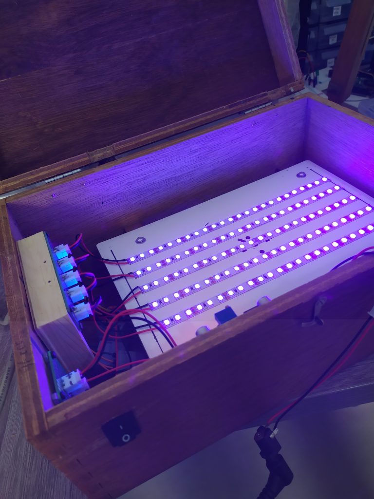
Homemade Bromograph Working
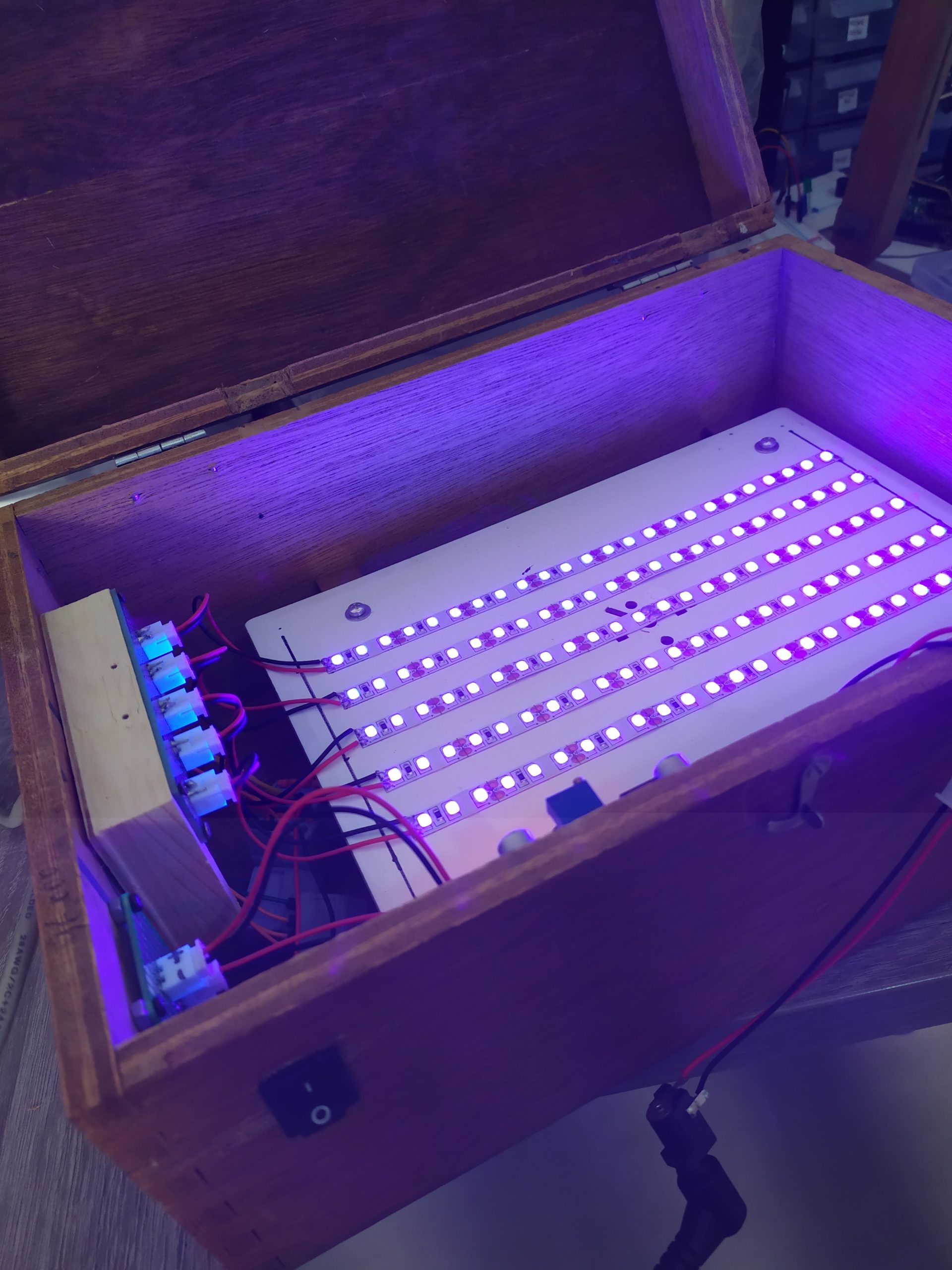
I used some connectors for the wiring and two diodes as a protection against polarity inversion but you can do without them. I had them so I used them.
For impressing the schematics on the copper board I tape the master printing on the board, put on the bromograph glass and then add 4 heavy books to keep nice and pressed and be sure the paper is flat against the board. The timing I use is 90 seconds, you can try with longer or shorter timings, what’s important is that you obtain a clear drawing on the board and, the lines must be solid and you can read the text.

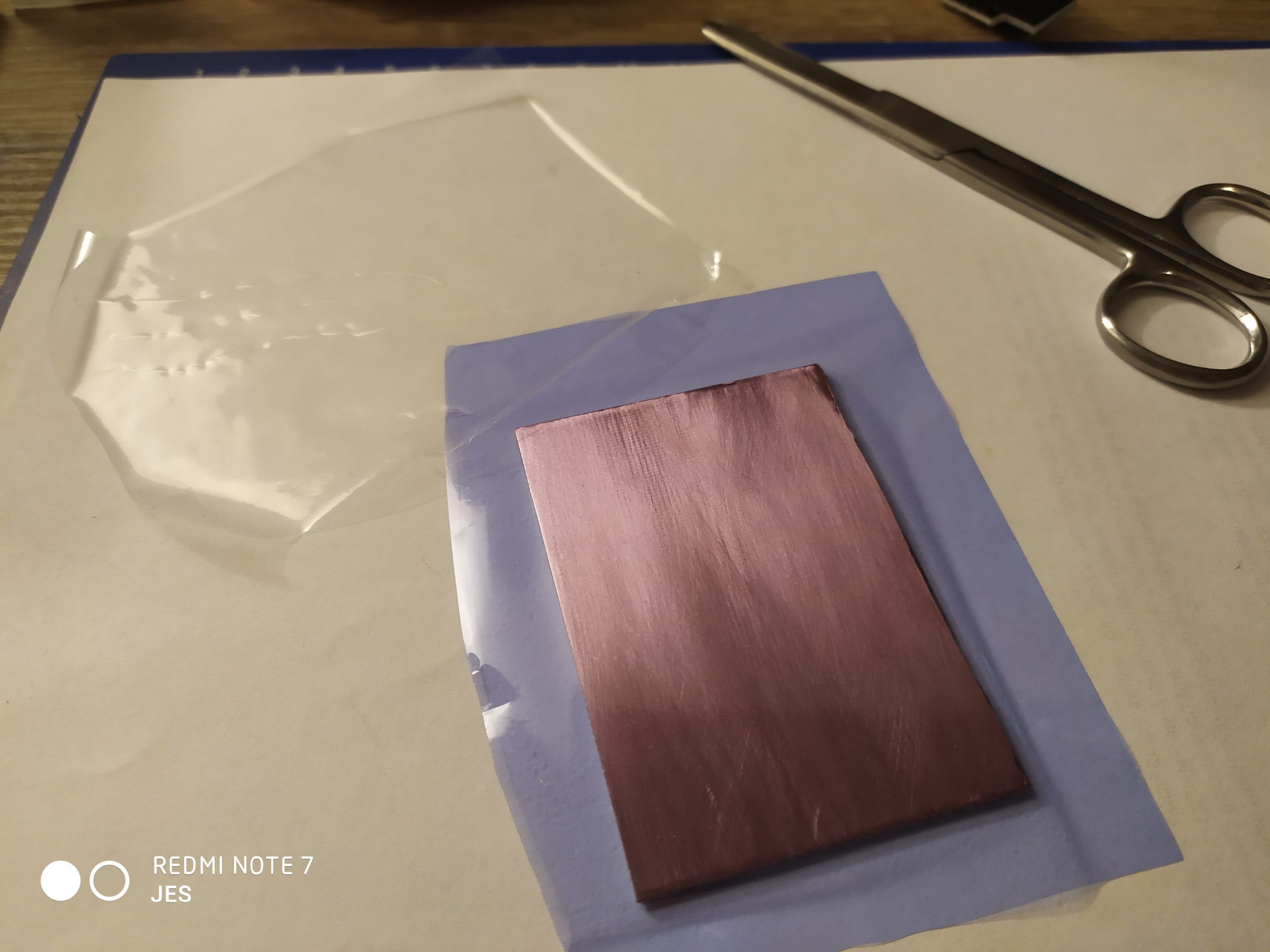
After Bromograph Impression 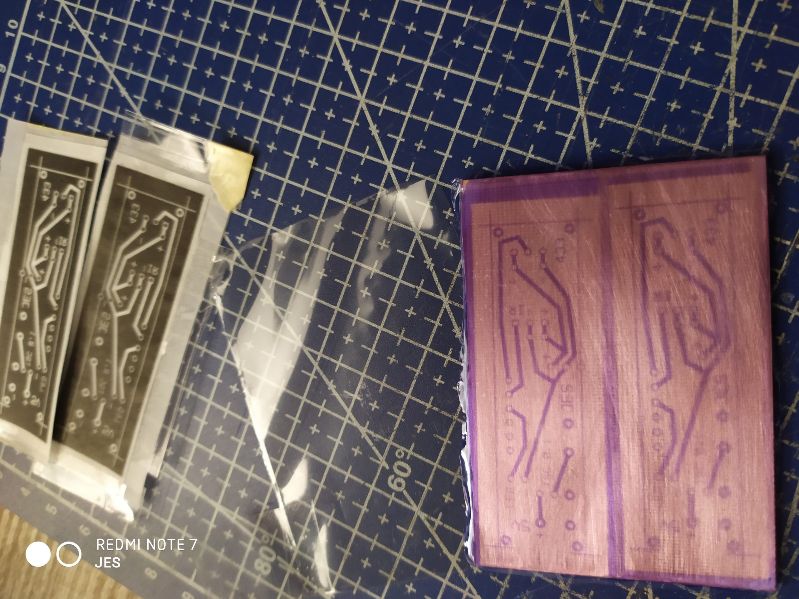
Remove Second Protective Film
Now we have the Dry Film impressed with the schematics. If the result isn’t good you can remove the part of the film by hand (it’s glued to the board in someway) and remove what’s left using pure acetone, and then start again with this same board.
Cut the margins off and there’s a second protective layer of the dry film to remove. This always takes me quite a bit of time because it’s very tricky to remove. We must not remove the dry film but only the transparent top protective layer. Again, I use two little squares of tape put on a corner of the dry film (one on top side of the film, one on the bottom) to remove this layer.
Next steps are with the chemical products to obtain the finished board by removing all the copper in excess. That will be published in part 2 of the article.
Enjoy!